
Nanotechnology is a rapidly growing field in the subject of Technology that deals with the manipulation of matter at the atomic and molecular scale. It enables the creation of new materials and devices with a wide range of applications in medicine, electronics, energy, and more.
This post is written for the RAS Mains examination; click here to read the short version for the RAS Prelims exam.
Nanotechnology
Definition and Basic Concept:
- Nanotechnology involves the study, manipulation, and application of materials at the nanoscale (1–100 nanometers / 10-9 – 10-7meters).
- At this scale, quantum effects and surface area-to-volume ratios dominate, leading to unique physical, chemical, and mechanical properties.
Understanding the Nanoscale
- Nanoscale Dimensions:
- 1 nanometer = one billionth of a meter (10⁻⁹ meters).
- Comparison:
- A sheet of paper is about 100,000 nm thick.
- A virus (~100 nm), DNA strand (~2 nm in diameter).
- A single human hair is about 80,000–100,000 nm wide.
- Properties of materials, such as color, reactivity, and strength, change due to nanoscale effects.
| Natural Nanomaterials | Synthetic Nanomaterials |
| Occur naturally in the environment. | Manufactured through controlled processes in labs. |
| May be less uniform in structure and properties. | Can be engineered to have specific properties and functions. |
| Examples include clay minerals, proteins, and natural fibers. | Examples include carbon nanotubes, gold nanoparticles, and quantum dots. |
Key Scientific Principles in Nanotechnology
Quantum Effects:
- At the nanoscale, materials exhibit quantum mechanical effects that are not observed at macroscopic sizes. This includes phenomena like:
- Quantum Confinement: Movement of electrons is restricted in one or more dimensions, leading to discrete energy levels. This affects the material’s electrical, optical, and magnetic properties.
- Optical Properties: Nanoscale materials may absorb and emit light differently, exhibiting color changes that bulk materials don’t. Example: Quantum dots glow in different colors depending on their size and are used in LED displays and medical imaging.[Smaller dots emit blue light, larger dots emit red].
- Electrical Properties: Electrons can “tunnel” through barriers at the nanoscale, contributing to conductivity in devices such as tunneling diodes and quantum dots.
- Magnetic Properties: Nanomaterials can show superparamagnetism, where they behave as magnets only when exposed to a magnetic field, but not after the field is removed. Example: Magnetic nanoparticles in MRI contrast agents.
- Quantum Confinement: Movement of electrons is restricted in one or more dimensions, leading to discrete energy levels. This affects the material’s electrical, optical, and magnetic properties.
Surface Area-to-Volume Ratio:
- Nanoparticles have a much higher surface area relative to their volume, enhancing their reactivity and strength.
- Example: Nanocatalysts (e.g., platinum or gold nanoparticles) are used in fuel cells and the automotive industry to speed up chemical reactions.
- Enhanced Strength: Materials at the nanoscale can be much stronger because of their structure (fewer grain boundaries, defects, and dislocations) and the greater interaction between surface atoms. For example: Carbon nanotubes (CNTs) are incredibly strong due to their atomic bonding, even though they are very light.
- Titanium dioxide nanoparticles exhibit better wear resistance, making them ideal for coatings used in cutting tools, electronics, and automotive parts.
- Improved Properties: improved solubility, better conductivity, and increased interaction with biological systems.
- Melting Point Reduction: At the nanoscale, the melting point of materials often decreases as particle size decreases.
- In nanoparticles, a large fraction of atoms are located on the surface compared to the interior. Surface atoms are less tightly bound because they have fewer neighboring atoms to stabilize them. As a result, less energy (heat) is needed to break the bonds and cause melting. Example: Gold:
- Bulk Gold→ 1064°C.
- 5 nm Gold particles → Melting point drops significantly.
- Capillary Forces: Capillary forces arise due to surface tension and are important at the nanoscale because the surface area is so large relative to the volume.
- Nanoscale Friction:
- Unlike bulk materials, friction at the nanoscale is governed by surface forces (e.g., van der Waals forces) and atomic interactions.
- The high surface-to-volume ratio of nanoparticles and nanosurfaces increases the contact area and the potential for friction. Even slight surface roughness can lead to significant friction at this scale.
- Managing and controlling friction at the nanoscale is essential for the development of advanced nanotechnology applications like MEMS, nanorobotics, and self-lubricating surfaces.
History and Development of Nanotechnology
- 1959 – Richard Feynman’s Vision: → Feynman’s lecture, “There’s Plenty of Room at the Bottom,” imagined manipulating atoms individually.
- 1974 – Norio Taniguchi: → Coined the term “nanotechnology” to describe precision machining at the nanometer scale.
- 1981 – Scanning Tunneling Microscope (STM):
→ Enabled visualization and manipulation of individual atoms. Gerd Binnig and Heinrich Rohrer of IBM received the Nobel Prize in 1986 for this. - 1985 – Discovery of Fullerenes:→The discovery of fullerenes (a new form of carbon) by Richard Smalley, Robert Curl, and Harold Kroto earned them the Nobel Prize in Chemistry.
- 1999 – First Molecular Machine:→ Development of a molecular-scale rotary motor, demonstrating molecular machines.
- 2000s-Present – Expanding Applications:→ Nanotechnology applied in medicine (drug delivery), electronics (nanotubes), and energy (solar cells, batteries).
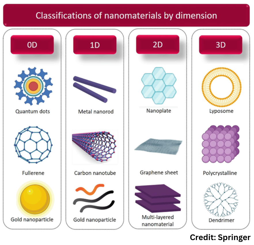
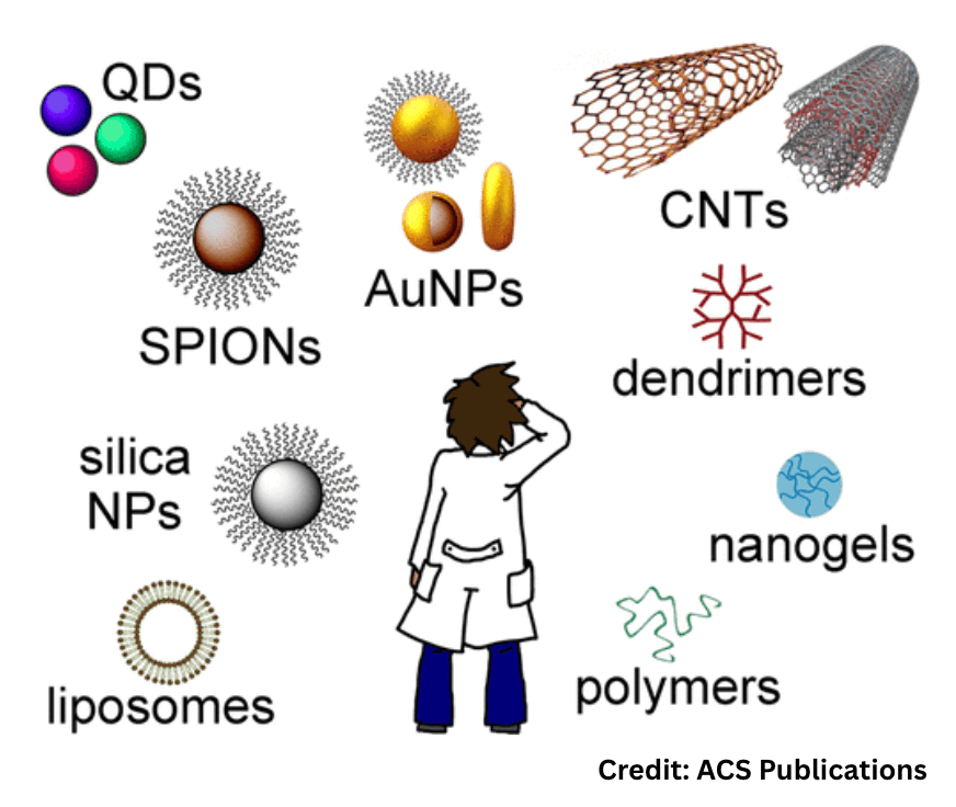
Types of Nanomaterials
A. Classification by Dimensions
1. Zero-Dimensional Nanomaterials (0D)
- Structure: Particles with all three dimensions in the nanoscale (e.g., nanoparticles).
- Examples:
- Quantum dots: Nanoscale semiconductor particles that exhibit unique optical properties.
- Fullerenes (C60): Molecules composed entirely of carbon atoms forming a hollow sphere, ellipsoid, or tube.
2. One-Dimensional Nanomaterials (1D)
- Structure: Materials with one dimension at the nanoscale (length), while the other two dimensions are larger.
- Examples:
- Nanotubes: Hollow cylindrical structures made of carbon (e.g., carbon nanotubes).
- Nanowires: Thin, wire-like structures of metals, semiconductors, or carbon.
- Nanorods: Rod-shaped nanomaterials that can be made from metals, oxides, or polymers.
3. Two-Dimensional Nanomaterials (2D)
- Structure: Materials with two dimensions at the nanoscale (length and width), but thickness is much smaller. They include nanosheets, nanofilms, and materials like graphene.
- Examples : Graphene – A single layer of carbon atoms arranged in a hexagonal lattice.
4. Three-Dimensional Nanomaterials (3D)
- Structure: These materials have all three dimensions larger than the nanoscale but may contain nanoscale features.
- Properties: Often exhibit higher porosity, large surface areas, and unique interactions with light or gases.
- Examples:
- Nanostructured films.
- Nanocomposites: Materials that combine nanoscale particles with a matrix material, resulting in enhanced properties (e.g., strength, conductivity).
B. Types Based on Composition
- Organic Nanomaterials/Carbon-Based Nanomaterials: Primarily composed of carbon, these include:
- Carbon Nanotubes (CNTs): Cylindrical structures with unique electrical properties.
- Fullerenes: Spherical or ellipsoidal forms of carbon.
- Inorganic Nanomaterials/Metal-Based Nanomaterials: Composed of metals:
- Nanosilver and Nanogold: Known for their antimicrobial properties.
- Quantum Dots: Semiconductor nanoparticles that exhibit quantum mechanical properties.
- Metal Oxides: Such as titanium dioxide nanoparticles, used in various applications including photocatalysis.
- Nanocomposites: Combinations of nanomaterials with other materials (eg. nanosized clays into plastics) to enhance properties like strength, conductivity, and flexibility.
- Dendrimers: These are branched polymers with a tree-like structure, useful in drug delivery and molecular recognition due to their high surface area and functionalization capabilities.
C. Special Types
- Nanoporous Materials: Contain nanopores and are used in applications like filtration and catalysis.
- Nanofibers: Fibrous nanomaterials, usually composed of polymers or carbon.
- Properties: High surface area and mechanical strength, used in filtration, textiles, and tissue engineering.
- Nanocapsules: : Hollow nanoparticles, typically used for drug delivery.
- Properties: Can carry drugs inside their core, releasing them in a controlled manner for targeted delivery.
- Nanofoams: Solid or liquid matrices filled with gas, useful in insulation and lightweight materials.
Nanofabrication Techniques
Top-Down Approach
- Starts with a bulk material and removes parts to achieve nanoscale dimensions. This is like “sculpting” at the atomic level.
- Key Techniques:
- Lithography: Used in electronics to etch nanoscale patterns on semiconductor chips. Common forms :
- Photolithography: Light-based patterning (e.g., used in microelectronics).
- Electron Beam Lithography (EBL): High-precision patterns (< 10 nm) using electron beams.
- X-ray Lithography: Finer features with X-rays (shorter wavelength).
- Etching: After lithography, etching removes unwanted material to define structures. Techniques include:
- Reactive Ion Etching (RIE)
- Wet Etching.
- Laser Ablation.
- Lithography: Used in electronics to etch nanoscale patterns on semiconductor chips. Common forms :
- Examples in Practice:
- Microchips and transistors in modern electronics.
- Nano-patterning for solar cells.
- Nano-coatings for improved durability and wear resistance.
- Advantages:
- High precision and control over nanoscale patterns.
- Suitable for large-scale production.
- Limitations:
- Wasteful: Involves removing material, leading to waste.
- Expensive: Requires sophisticated tools and facilities.
Bottom-Up Approach
- Starts at the atomic or molecular level to build nanoscale structures through self-assembly or chemical synthesis. This is like “building” nanoscale objects atom by atom.
- Key Techniques:
- Self-Assembly: Molecules or atoms organize themselves into predefined structures due to natural forces. Example: Nanocrystals, block copolymers, DNA nanotechnology.
- Chemical Vapor Deposition (CVD): Deposits thin films/nanostructures using gaseous reactants. Example: Carbon nanotubes, graphene synthesis.
- Atomic Layer Deposition (ALD): Alternating chemical reactions deposit one atomic layer at a time.
- Epitaxial Growth: Deposits material layers on crystalline substrates with controlled orientation. Example: LED manufacturing.
- Colloidal Synthesis: Produces nanoparticles like quantum dots through controlled chemical reactions.
- Examples in Practice:
- Fabrication of quantum dots used in medical imaging and displays.
- Carbon nanotubes for stronger materials.
- Drug delivery systems using nanocarriers.
- Advantages:
- Minimal waste: Builds materials directly at the nanoscale.
- Enables complex and intricate structures.
- Limitations:
- Less precise compared to Top-Down.
| Aspect | Top-Down | Bottom-Up |
| Process | Subtractive (removal of material). | Additive (building from atoms/molecules). |
| Precision | High precision in patterning. | Intricate structures but less precise. |
| Waste | Generates material waste. | Minimal waste. |
| Applications | Electronics (chips, circuits). | Drug delivery, quantum dots, carbon nanotubes. |
| Cost | High due to expensive equipment. | More cost-effective for complex structures. |
| Scalability | Suitable for mass production. | Difficult to scale industrially. |
Applications of Nanotechnology
Medicine and Healthcare
- Drug Delivery: Nanocarriers (liposomes, dendrimers) for targeted drug delivery.
- Medical Imaging:
- Iron oxide nanoparticles → Enhanced MRI contrast for better diagnosis
- Quantum dots → Sensitive fluorescence imaging
- Diagnostics:
- Nano biosensors → Rapid biomarker detection
- Gold nanoparticles are used in pregnancy tests and detecting biomarker proteins.
- Tissue Engineering:
- Nanofibers like polycaprolactone (PCL), collagen are used to create scaffolds for tissue regeneration, guiding cell growth.
- Antimicrobial Coatings: Nanosilver, nanocopper, and zinc oxide. Example:
- Silver nanoparticles are used in wound dressings and surgical instruments to prevent infections.
- Copper nanoparticles are used in disinfectant sprays and hospital surfaces.
- Wound Healing:
- Nanoparticle-loaded hydrogel → Faster healing
- Cancer Treatment
- Gold nanoparticles → Targeted chemotherapy
- Vaccine Delivery: Biodegradable nanoparticles, liposomes, and micelles for controlled antigen release, enhancing vaccine delivery and stability.
- Nanobots: Nano-sized robots for targeted drug delivery, microsurgeries, and diagnostics inside the body
Challenges and Safety Concerns
- Blood-Brain Barrier: Nanoparticles struggle to cross the blood-brain barrier → Limits neurological applications
- High Costs: Expensive production processes → Limits accessibility and mainstream use.
- Toxicity: Potential for nanoparticles to cause oxidative stress, inflammation, DNA damage
- Bioaccumulation: Nanoparticles may accumulate in organs like liver, spleen, lungs → Long-term effects unknown.
- Environmental Toxicity: Release of nanoparticles into the environment → Potential risk to aquatic & terrestrial life.
Future
- Targeted Gene Therapy: Liposomes or nanoparticles for DNA/RNA delivery → Correct genetic defects
- Nano-Vaccines: Nanocarriers, microneedle arrays → Improved vaccine delivery systems
- Photothermal Therapy: Carbon nanotubes → Use light absorption to destroy cancer cells via heat
- Personalized Medicine: Nanosensors + AI for tailored treatment based on individual genetic data.
Electronics and IT
- Smaller Devices: Carbon nanotubes (CNTs), graphene, and quantum dots enable the miniaturization of electronic components.
Example: Carbon nanotube transistors in processors. - Flexible Electronics: Flexible OLED screens made from graphene are used in smartphones, tablets, and wearables.
- High-Performance Batteries: Silicon nanoparticles, graphene for better energy storage. Example: Silicon anode-based lithium-ion batteries offer higher energy storage capacity, reducing battery size and weight.
- Quantum Computing: Quantum dots, nanowires, and nanomagnets are used to create qubits for quantum computing.
Energy
- Solar Cells: Perovskite nanomaterials, quantum dots, and TiO2 nanomaterials improve light absorption and conversion efficiency in solar cells.
- Fuel Cells: Nanocatalysts (platinum nanoparticles) for improved reactions. Example: Platinum nanoparticles improve the catalytic reaction rates in hydrogen fuel cells.
- Energy Storage: Graphene-based supercapacitors are used to enhance energy storage in electric vehicles (EVs) by providing rapid charging and discharge.
- Wind Turbines: Nanocoatings for improved durability. Example: Graphene coatings on turbine blades.
- Tiny carbon ‘flowers’ turn light to heat at unrivalled efficiency.
Environment
- Water Purification: Nanomembranes, titanium dioxide (TiO2) nanoparticles, and nanocatalysts are used to purify water..
- Air Filtration: Nanofibers, carbon nanotubes for pollutant removal. Example: Nanofiber air filters for PM2.5.
- Waste Management: Nanocatalysts, nanomaterials, and nano-adsorbents break down or capture toxic chemicals from industrial waste and pollutants. Example: Nano-structured iron oxide for wastewater treatment.
- Sustainable Agriculture: Nano-enabled fertilizers for better crop yield. Example: Nano-silver fertilizers to promote plant growth.
Nanobubble Technology
Nanobubbles are extremely tiny gas bubbles, smaller than a virus (less than 200 nanometers). Unlike regular bubbles that float to the surface and burst, nanobubbles stay suspended in water for a long time due to their unique properties.
Working Principle:
- Stability: Nanobubbles possess a strong negative charge, which helps them attract and break down impurities in the water.
- High Surface Area: Their small size gives them a large surface area, making them efficient for gas exchange (e.g., oxygen dissolves better in water).
Why Nanobubbles Are Useful
- They improve water quality by oxygenating it and removing harmful substances.
- They are eco-friendly, as they don’t rely on harmful chemicals.
- Their versatility makes them useful in multiple fields like agriculture, water treatment, aquaculture, and even medicine.
Recently, the National Zoological Park in Delhi initiated a 15-day trial of Nano Bubble Technology to improve water quality in its ponds.
Aerospace and Automotive
- Lightweight Materials: Carbon nanotubes (CNTs), graphene, and nanocomposites reduce the weight of components while enhancing their strength and durability.
- Lubricants and Coatings: Nanocoatings like graphene and nanodiamond films reduce friction and wear in automotive and aerospace components.
- Sensors: Nanowires, CNTs for monitoring engine and environmental conditions.
Textiles
- Smart Fabrics: Nanocoatings like silver nanoparticles and nano-zinc oxide provide textiles with properties like water resistance, stain resistance, and UV protection.
- Example: Nano-silver-treated fabrics offer antibacterial protection in hospital garments and sportswear.
- Antimicrobial Properties: Titanium dioxide, nanosilver for fabric hygiene. Example: TiO2 nanoparticles in hospital textiles.
Cosmetics and Personal Care
- Sunscreens: Nano-sized titanium dioxide, zinc oxide for UV protection.
- Skin Care: Nanocarriers (liposomes) for deeper ingredient absorption. Example: Liposome-based skin moisturizers.
- Hair Care: Nanocapsules in hair care products deliver vitamins and essential oils to nourish hair.
Defense and Security
- Protective Gear: Kevlar, carbon nanotubes for stronger, lightweight armor.
- Detection Systems: Nanosensors for detecting explosives, toxins. Example: Graphene-based biohazard detection sensors.
- Stealth Technology: Carbon nanotube-based coatings reduce radar visibility for aircraft and vehicles.
Construction and Infrastructure
- Cement and Concrete:Nanoparticles like silica fume and titanium dioxide enhance concrete strength and reduce cracks.
- Example: Nano-silica is added to concrete to increase its tensile strength and durability.
- Coatings: Self-cleaning nanocoatings are used on building windows to resist dirt and water.
- Energy-Efficient Buildings: Aerogel insulation reduces energy loss in buildings, improving efficiency.
- Sports Equipment: Nano-reinforced materials make equipment like tennis rackets, golf balls, and bicycles stronger and lighter.
Food and Agriculture
- Faster Seed Germination: Nano priming of seeds with materials like zinc and titanium dioxide speeds up germination and growth.
- Nano porous zeolite → improve water holding capacity of soil
- Nano-fertilizers: Deliver nutrients efficiently and reduce wastage. Example:
- Nano-urea developed by IFFCO improves nitrogen absorption.
- Zinc oxide (ZnO) nanoparticles for crop fortification.
- Nano-pesticides: Target pests with precision, minimizing environmental damage. Example:
- Nano-silver pesticides for controlling fungal infections.
- Nanocapsules containing neem oil for bio-pesticidal applications.
Nano Urea
- Nano Urea: A novel form of liquid urea fertilizer developed using nanotechnology.
- It involves breaking down urea into nanoscale particles (less than 100 nanometers). These tiny particles enhance nutrient absorption by plants.
Key Features:
- Concentration: 40,000 mg/L of nitrogen.
- Equivalent: 500 ml bottle = 1 bag (50 kg) of traditional urea.
- Application: Foliar spray for better absorption.
How It Works
- Encapsulation: The nitrogen in traditional urea is encapsulated in nanoparticle forms, which slowly release nutrients to plants over time.
- Foliar Spraying: This direct foliar application increases nutrient absorption through stomata, ensuring efficient utilization.
Advantages Over Traditional Urea
- Increased Efficiency: Effectiveness >80% vs. 30-40% for conventional urea.
- Reduced Quantity Required: Use at least 50% less than traditional urea.
- Environmental Benefits: Minimizes runoff and pollution.Helps reduce greenhouse gas emissions.
- Enhanced Crop Yield: Average yield increase of ~ 8% in trials.
Development and Research
- Developed by IFFCO at its Nano Biotechnology Research Centre, Gujarat.
Nano Urea = Efficient, eco-friendly, and cost-effective fertilizer for sustainable agriculture.
Precision Farming
- Nanosensors: Monitor soil health, moisture levels, and nutrient content. Example: Soil nano-sensors used to detect pH, salinity, and nutrient deficiencies.
Water Management
- Nano-enabled Water Purification: Nanofilters and membranes remove contaminants like heavy metals, pathogens, and salts.
- Nano-coatings: Hydrophobic coatings for soil to improve water retention.
Sustainable Agriculture
- Nano-coatings: Protect seeds and enhance germination. Example: Nano-polymer coatings on seeds improve germination and drought resistance.
- Clay Nanoparticles: Incorporating clay nanoparticles into soil enhances its structure, water retention, and nutrient-holding capacity
- Controlled Release of Inputs: Nanoparticles ensure slow, sustained release of nutrients. Example: Nano-clay for controlled fertilizer release.
Post-Harvest Management
- Nano-packaging: Extends shelf life of food by preventing spoilage.Example: Nano silver coated storage bags to prevent microbial growth.
- Nano-sensors: Detect ripeness, spoilage, or contaminants in stored produce. Example: Sensors to monitor ethylene gas levels in stored fruits.
Pest and Disease Control
- Nanoparticles: Target pests and diseases without harming crops. Example: Zinc oxide and copper nanoparticles combat bacterial and fungal diseases.
Nanotechnology in Genetic Engineering
- Nanocarriers transport genes or biomolecules into plants more efficiently. → Development of genetically modified crops with improved traits like drought tolerance and pest resistance.
Irrigation Automation
- Nano Ganesh: An irrigation automation system that allows farmers to remotely control irrigation pumps using mobile phones
Food Packaging:
- Nanosensors, nanocoatings for spoilage detection and contamination prevention. Example: Nano-silver in packaging.
Food Safety
- Example: Magnetic nanoparticles for detecting pathogens like Salmonella and E. coli.
Nutrient Delivery:
- Nanoencapsulation for targeted nutrient release.
Example: Nanoencapsulated vitamin A in food products
Smart Packaging
- Spoilage Detection: Packaging integrated with nanosensors detects gases released during food spoilage and changes color to indicate freshness.
- Example: Colour-Changing Packaging helps monitor food quality during storage.
Meat Processing
- Antimicrobial coatings (Silver, magnesium oxide, chitosan) → Reduce biofilm formation
Bakery Products
- Dough conditioning → Zinc oxide nanoparticles Improve handling properties
Horticulture
- Aloe vera nanofibers based coating → Reduce moisture loss
Beverages
- Toxin detection thorough Gold nanoparticles → Sense contaminants in beverages
Challenges:
- Toxicity Concerns → Requires evaluation of environmental and health impact
- High Costs → Investment in R&D needed
- Regulations → Need for clear guidelines
- Lack of Awareness → Educating farmers and industries on benefits.
Government Initiatives on Nanotechnology in Agriculture
- Nano Mission: Research centres like IISc Bangalore focus on nano-fertilizers and food packaging
- National Agricultural Innovation Project (NAIP) : Projects to explore nanotechnology inn agriculture
- ICAR Initiatives: Nanotechnology Centres for developing nano-biosensors and nano-pesticides
- IFFCO’s Nano Urea: First in the world to produce Nano Urea, reducing soil and environment degradation
- International Collaboration: Indo-UK project on nano-sensors for soil and crop health
Future Possibilities:
- Nano Tech + AI-driven automation → Advanced precision farming
- Smart nano-pesticides → Sustainable agricultural practices
- Nano-enabled Urban Agriculture → Vertical farms and nano-greenhouses for maximum productivity
- Active Packaging with Colour-changing Nanosensors → Visual spoilage alerts for consumers.
Popular Nanomaterials
Silver Nanoparticles(Ag-NPs)
- Composition: Pure silver or silver oxide.
- Properties of Silver Nanoparticles
- Strong Antimicrobial Properties.
- Unique optical characteristics are utilized in sensors and imaging.
- AgNPs have high electrical conductivity, beneficial in electronic applications.
Applications
- Medical Applications:
- Antimicrobial Therapy → Used in wound dressings & medical devices to prevent infections
- Cancer Treatment → Investigated for targeting & treating cancer cells
- Food Industry:
- Packaging → Used in food packaging to extend shelf life by preventing bacterial growth
- Consumer Products:
- Textiles → Added to fabrics for antimicrobial properties
- Cosmetics → Used in creams & lotions for antibacterial effects
Gold nanoparticles (AuNPs)
Unique Properties:
- Small Size (1-100 nm) → High surface area-to-volume ratio → Increased reactivity & interaction with biological molecules
- Optical Properties → Strong light absorption & scattering → Vibrant colors (red to purple) due to surface plasmon resonance (SPR)
- Biocompatibility → Non-toxic & biocompatible → Suitable for biomedical uses (drug delivery, cancer therapy, imaging)
Medical Applications:
- Diagnostics → Used in biosensors & imaging for enhanced medical visualization
- Drug Delivery → Carries drugs, DNA to targeted diseased cells
- Therapeutics → Photothermal therapy for cancer treatment (converts light to heat to destroy cancer cells)
- Cosmetics → Antioxidant & anti-aging properties in skincare products
Recent Development:
- Cordy Gold Nanoparticles (Cor-AuNPs) → Enhances drug delivery systems.
Carbon Nanomaterials
Materials made of carbon atoms arranged in different shapes, such as tubes or sheets.
A. Carbon Nanotubes
Carbon Nanotubes (CNTs) are cylindrical nanostructures composed of rolled-up sheets of single-layer carbon atoms(graphene) in a hexagonal lattice.
Properties of Carbon Nanotubes (CNTs):
- Strength → 100x stronger than steel but lightweight
- Conductivity → Excellent conductor of electricity & heat (ideal for electronics & energy applications)
- Flexibility → Can bend without breaking
- High Surface Area → Ideal for energy storage & sensor applications
Types of CNTs:
- Single-Walled Carbon Nanotubes (SWCNTs) → One tube of carbon atoms, highly conductive & flexible
- Multi-Walled Carbon Nanotubes (MWCNTs) → Multiple layers of nanotubes, stronger but less conductive
Applications of CNTs:
- Electronics: Used in transistors to improve speed & energy efficiency → Faster, more efficient electronics
- Energy Storage: Used in batteries & supercapacitors → Longer-lasting energy storage (mobile phones, electric cars)
- Medical Applications : Used in Targeted medicine delivery, reducing side effects
- Material Strength: Added to composites like carbon fiber for stronger, lighter materials → Used in airplanes, spacecraft, sports equipment
- Water Purification: Acts as a nano-sieve to filter impurities from water → More efficient water cleaning, especially in low-quality water areas
- Sensors: Sensitive to gases & chemicals for pollutant, toxin, or disease detection → Early disease detection & environmental monitoring.
Challenges with CNTs:
- Cost → Expensive production limits widespread use
- Health & Safety → Potential respiratory issues if inhaled (ongoing research)
- Scalability → Difficulty in producing large, consistent quantities at low cost.
B. Graphene
Graphene is a single layer of carbon atoms arranged in a honeycomb-like structure. It’s like a super-thin sheet of carbon(two-dimensional material), just one atom thick!
Properties of Graphene:
- Super Strong → 200x stronger than steel, lightweight & flexible
- Excellent Electrical Conductivity → Better than copper, ideal for electronics
- Superb Thermal Conductivity → Efficient heat conduction
- Transparency → Almost transparent, useful for touch screens
- High Surface Area → Allowing for high storage capacity, great for batteries & sensors
Applications of Graphene:
- Electronics & Computers: Used in transistors to create faster, energy-efficient devices → Boosts speed and power in electronics
- Energy Storage (Batteries & Supercapacitors): Used in batteries and supercapacitors for higher energy storage → Longer-lasting, faster-charging batteries (phones, electric cars)
- Medical Applications : Used in drug delivery systems for precise, targeted treatments
- Water Filtration: Graphene oxide membranes filter water at the molecular level
- Sensors : Graphene sensors detect gases, chemicals, and diseases →Detects small quantities for environmental & medical monitoring
- Super Strong Materials: Strengthens plastics for use in aerospace, construction, & sports equipment → Lightweight, strong materials for demanding applications
- Transparent Touchscreens: Used in touchscreen displays as a transparent conductor
Graphene is often referred to as a “wonder material” because it could revolutionize many industries, making things stronger, faster, and more efficient.
C. Fullerenes (C60)
- Structure: Spherical molecules of carbon atoms arranged in a soccer-ball-like pattern (20 hexagons + 12 pentagons).
- Composition: 60 carbon atoms (C60), also called “buckyballs.”
Unique Properties of Fullerenes
- Spherical Shape: Hollow, cage-like structure provides high stability.
- Electrical Conductivity: Function as conductors, semiconductors, or insulators based on modifications
- High Strength: Lightweight yet mechanically robust
- Chemical Stability: Resistant to degradation under normal conditions.
- Electron Acceptors: Useful in electronics and photovoltaics.
- Antioxidant Properties: Neutralize free radicals, beneficial in medical applications.
Applications of Fullerenes (C60)
1. Medicine
- Drug Delivery: Encapsulate drugs, delivering them to targeted cells (e.g., cancer treatment).
- Antiviral/Antibacterial Agents: Potential to inhibit HIV replication and fight infections.
- Antioxidants: Combat oxidative stress, benefiting arthritis, neurodegenerative diseases, and aging-related conditions.
2. Energy and Electronics
- Solar Cells: Act as electron acceptors in organic photovoltaic cells, enhancing efficiency.
- Batteries: Improve lithium-ion battery capacity and durability.
- Superconductors: Modified fullerenes exhibit superconducting properties at low temperatures.
3. Environmental Applications
- Water Purification: Trap and remove pollutants and toxins.
- Air Purification: Under exploration for capturing pollutants like CO2.
4. Material Science
- Nanocomposites: Strengthen polymers for aerospace and automobile industries.
- Lubricants: Spherical shape reduces friction, ideal as nano-lubricants.
5. Cosmetics
- Anti-Aging Products: Antioxidant properties reduce wrinkles and skin damage.
Facts
- Discovery: Found in 1985 by Curl, Smalley, and Kroto, who won the Nobel Prize in Chemistry in 1996.
- Name Origin: Inspired by Buckminster Fuller’s geodesic dome designs.
- Space Connection: Fullerenes detected in outer space suggest a cosmic origin.
Quantum Dots
Quantum dots (QDs) are nanoscale semiconductor particles, typically ranging from 2 to 10 nanometers in size, that exhibit unique optical and electronic properties due to quantum mechanical effects.
- These particles are often referred to as “artificial atoms” because their behavior is governed by the principles of quantum physics.
Properties of Quantum Dots:
- Size-Dependent Properties → The size of a quantum dot determines its color: smaller dots emit blue light, larger dots emit red light.
- Bright and Stable Light Emission → Emit stable, bright light over time, ideal for displays & imaging.
- Tunable Emission → Color of light emitted can be tuned by adjusting the size of the quantum dot.
- Strong Absorption → Can absorb a wide range of light wavelengths (UV to visible) and convert them into specific colors.
Applications of Quantum Dots:
- Displays and TVs: Used in quantum dot displays (e.g., LED TVs) → Provide brighter colors and better energy efficiency, improving image quality and reducing power use.
- Biomedical Imaging: Used for tracking cells or molecules in the body, especially in cancer diagnosis. → Bright and stable light emission helps detect diseases at early molecular stages.
- Solar Cells: Can increase solar energy efficiency, making it cleaner and more affordable.
- Sensors: Highly sensitive sensors for environmental monitoring and medical diagnostics.
- Quantum Computing (Future): Quantum dots could be key in developing quantum computers.
Challenges of Quantum Dots:
- Toxicity → Some QDs contain toxic materials (like cadmium), raising environmental and health concerns.
- Manufacturing Difficulties → Producing high-quality, uniform quantum dots in large quantities is challenging and costly.
- Cost → High production costs limit widespread adoption.
Recent Developments
- In 2023, the Nobel Prize in Chemistry was awarded to Moungi G. Bawendi, Louis E. Brus, and Alexei I. Ekimov for the discovery and synthesis of quantum dots.
Zinc Oxide (ZnO) Nanoparticles
Uses:
- Sunscreens (to protect from UV rays).
- Medicine (to treat skin conditions).
- Electronics (in LED lights and solar cells).
Magnesium Oxide (MgO) Nanoparticles
Magnesium Oxide Nanoparticles are used for environmental purposes like cleaning water, removing harmful pollutants, and acting as antimicrobial agents to kill germs.
Uses:
- Water treatment (to purify water).
- Medicine (to treat acidity and heartburn).
- Environmental protection (to remove pollutants).
Silica Nanoparticles
These are tiny particles made of silicon dioxide (a compound found in sand).
Uses:
- Drug delivery (to target specific areas in the body).
- Cosmetics (for smoother textures in creams and powders).
- Food (as an anti-caking agent in powdered foods).
Titanium Dioxide (TiO2) Nanoparticles
Uses:
- Sunscreens (for UV protection).
- Paints and coatings (for bright colors and durability).
- Self-cleaning surfaces (for windows, tiles).
Challenges and Ethical Issues
- Health and Safety Risks
- Unintended Effects on Health: Nanomaterials are so small that they can easily penetrate the skin, lungs, and other organs, potentially causing harm to cells and tissues.
- Toxicity : Carbon nanotubes are known to cause inflammation in animal studies.
- Environmental Impact
- Bioaccumulation: Silver nanoparticles, used in antimicrobial products, can accumulate in fish and other aquatic organisms.
- Pollution: Nanoparticles from industrial waste could contaminate water sources.
- Privacy Concerns: Nano-surveillance tools (Nano-biosensors) used in health monitoring could track real-time biological data.
- Regulation & Oversight: Lack of consistent global standards and regulations for nanomaterials.
- Economic & Social Impacts: Risk of job displacement and unequal access to technology.
- Dual-Use Concerns: Potential for nanotechnology(Nanobots) to be used for harmful military applications.
- Ethical Treatment of Nano-Enhanced Organisms: Issues surrounding the modification of life forms using nanotechnology.
- Public Perception: Fear and misunderstanding of nanotechnology’s risks and benefits.
- Scalability: Difficulty in commercial-scale production of nanomaterials.
- Interdisciplinary Collaboration: Requires synergy across physics, biology, chemistry, etc.
- Intellectual Property (IP): Complex patenting and ownership issues.
Government Initiatives
2000s – Present
- 2001: Nano Science and Technology Initiative (NSTI)
- Launched under the Department of Science and Technology (DST) with an initial funding of Rs. 60 crores.
- Aimed to build research infrastructure and promote basic research in nanoscience.
- 2002-2007: Tenth Five-Year Plan:
- Recognized the need for a dedicated Nanomaterials Science and Technology Mission (NSTM).
- 2007: National Mission on Nano Science and Technology (Nano Mission)
- Launched by: Department of Science and Technology (DST), Government of India.
- Budget: Rs 1,000 crores allocated for five years.
- Objective: To promote basic research, develop infrastructure, and facilitate application-driven R&D in nanoscience and nanotechnology.
- Key Features:
- Funding for universities, R&D labs, and industry collaborations.
- Support for human resource development through fellowships, training, and international exchange programs.
- Development of state-of-the-art infrastructure like National Centres for Nanoscience and Nanotechnology.
- Promotion of public-private partnerships for technology commercialization.
- Achievements:
- Positioned India among the top five countries globally in nanoscience publications.
- More than 1000 research papers published annually under Nano Mission projects.
- Establishment of advanced research centers like the Centre for Nano and Soft Matter Sciences (CeNS) in Bengaluru.
- Established national centers for nanofabrication and nanoelectronics at institutions like IIT Bombay and IISc Bangalore.
- 2012-2017 (Phase II of Nano Mission): Twelfth Five-Year Plan
- Continued support for the Nano Mission with a budget of Rs. 650 crores
- Present : National Programme on Nano Science and Technology
- National Mission on Nano Science and Technology stands completed as on 31st March 2017.
- The above Mission has been converted to a National Programme on Nano Science and Technology.
- Research and Applications: India has seen over 13,350 nanotechnology patents granted since the inception of these initiatives.
Ministry of Electronics and Information Technology (MeitY) Initiatives:
- Established major Nanoelectronics Centres at premier institutes (IISc, IITs).
- Implemented the Indian Nanoelectronics Users Programme (INUP-i2i) to provide access to state-of-the-art nanofabrication facilities.
India’s Contributions in Nanotechnology
Research and Development
- India ranks among the top 5 countries globally in nanotechnology research publications.
- Recent Innovations and Focus areas
- C.N.R. Rao: Known as the “Father of Indian Nanotechnology” for contributions to carbon and inorganic nanotubes.
- Nanomedicine: Research on drug delivery systems, cancer therapy (e.g., nano-gold for tumor targeting).
- Agriculture: Development of nano-urea for sustainable farming.
- Water Purification: Carbon Nanotube Filters (BHU) remove nano-scale contaminants like E. coli and polio viruses.
- Healthcare Solutions: Defence Research & Development Establishment (DRDE), Gwalior developed a rapid typhoid detection kit using nanotechnology (1-3 minutes).
- Energy Generation: IISc, Bangalore developed self-powering pacemakers using electricity generated by liquid flow in carbon nanotubes.
Collaboration and Global Partnerships
- Collaborations with Countries: Partnership with USA, Germany, and Japan for advanced nanotechnology research.
- Bilateral agreements under initiatives like Indo-US Nanotechnology Forum.
- Participation in International Conferences:
- India is an active participant in forums like International Conference on Nanoscience and Technology (ICONSAT).
Make in India and Atmanirbhar Bharat:
- Promoting indigenous nanotechnology applications for self-reliance.
Way Forward
- Safety Measures: Rigorous testing of nanomaterials for health and environmental risks.
- Ethical Use: Ensure equitable distribution and ethical development of nanotechnology.
- Regulations: Develop clear frameworks and international standards.
FAQ (Previous year questions)
- Nanomaterials are materials with structures at the nanoscale, typically less than 100 nanometers.
- At this scale, they exhibit unique properties that differ significantly from their bulk counterparts, including enhanced mechanical, optical, electrical, and chemical characteristics.
- The fascination with nanomaterials largely stems from the unique quantum and surface phenomena that emerge at the nanoscale.
Two Carbon Allotropes Used as Nanomaterials:
- Graphene:
- Structure: Graphene is a single layer of carbon atoms arranged in a two-dimensional honeycomb lattice.
- Properties: It is incredibly strong (200 times stronger than steel), lightweight, tougher than diamond, and an excellent conductor of electricity and heat.
- Applications:
- Graphene’s high electrical conductivity makes it ideal for creating faster and more efficient transistors.
- Energy storage Devices : Graphene improves lithium-ion batteries and supercapacitors.
- Reinforced Materials: It enhances the strength and durability of composite materials used in the automotive, aerospace, and construction industries.
- Medicine: It aids in targeted drug delivery and advanced imaging techniques.
- Water Filtration: Used in membranes for water desalination and filtration due to its high permeability and selectivity.
- Quantum Computing: It holds potential for use in quantum computing for developing qubits.

- Carbon Nanotubes (CNTs):
- Structure: Carbon nanotubes are cylindrical nanostructures with a diameter in the nanometer range and lengths up to several micrometers. They can be single-walled (SWCNTs) or multi-walled (MWCNTs).
- Properties: They are lightweight, almost 1/6th the weight of steel, with a mechanical tensile strength nearly 400 times that of steel. They also possess extraordinary electrical conductivity and thermal conductivity. CNTs exhibit unique electronic properties that can be metallic or semiconducting, depending on their structure.
- Applications: CNTs are used in reinforcing materials to improve strength and durability, in electronic components like transistors and sensors, in energy storage devices, and in medical applications for drug delivery and imaging.
- CNTs are mixed with other materials to make composites like conductive plastics or steel-like plastics.
- The hollow, tubular structure makes CNTs ideal for storing gases, lithium, or even drugs.
- CNTs can be made into artificial blood capillaries to help injured parts of the human body.
- They can act as carriers for drugs and antigens in the human body.
- CNTs are used in electric wires to reduce losses and can also be used in solar cells.
National Mission on Nano Science and Technology (Nano Mission)
- Launched by: Department of Science and Technology (DST) of the Ministry of Science in 2007.
- Leadership :The Nano Mission Council (NMC) directs the Nano Mission under the leadership of Professor C.N.R. Rao.
- Budget: Rs 1,000 crores allocated for five years.
- Objectives:
- Foster basic research in nanoscience through funding and institutional support.
- Develop technological infrastructure and establish advanced research facilities.
- Promote human resource development through training and capacity building.
- Encourage public-private partnerships for translation of research into commercial applications.
- International Collaborations: Foster partnerships with global institutions.
- Phases: 2
- 1st Phase : 2007-2012
- 2nd Phase : 2012-2017
- The Nano Mission was completed on March 31, 2017, and was converted into the National Programme on Nano Science and Technology (NPNST).
- Achievements:
- Positioned India among the top five countries globally in nanoscience publications.
- More than 1000 research papers published annually under Nano Mission projects.
- Establishment of advanced research centers like the Centre for Nano and Soft Matter Sciences (CeNS) in Bengaluru.
- Established national centers for nanofabrication and nanoelectronics at institutions like IIT Bombay and IISc Bangalore.
- Size of Nanoparticles: Nanoparticles are particles with a size range of 1 to 100 nanometers (nm).
- Uses of Nanoparticles:
- Medicine: Targeted drug delivery and cancer treatment using nano-carriers.
- Electronics: Used in semiconductors and high-performance batteries. For example, quantum dots used in LED TVs and solar cells.
- Environment: Water purification through nano-filters and pollutant removal.
- Textiles: Antibacterial coatings (e.g., Nanosafe by IIT Delhi) and stain-resistant fabrics.
- Agriculture: Nano-fertilizers and pesticides for efficient nutrient delivery (Eg.Nano-urea by IFFCO).
Nanomaterials are materials with structures at the nanoscale, typically less than 100 nanometers.
At this scale, they exhibit unique properties that differ significantly from their bulk counterparts, including enhanced mechanical, optical, electrical, and chemical characteristics.
The fascination with nanomaterials largely stems from the unique quantum and surface phenomena that emerge at the nanoscale.
Two Carbon Allotropes Used as Nanomaterials:
Graphene:
Structure: Graphene is a single layer of carbon atoms arranged in a two-dimensional honeycomb lattice.
Properties: It is incredibly strong (200 times stronger than steel), lightweight, tougher than diamond, and an excellent conductor of electricity and heat.
Applications:
Graphene’s high electrical conductivity makes it ideal for creating faster and more efficient transistors.
Energy storage Devices : Graphene improves lithium-ion batteries and supercapacitors.
Reinforced Materials: It enhances the strength and durability of composite materials used in the automotive, aerospace, and construction industries.
Medicine: It aids in targeted drug delivery and advanced imaging techniques.
Water Filtration: Used in membranes for water desalination and filtration due to its high permeability and selectivity.
Quantum Computing: It holds potential for use in quantum computing for developing qubits.
Carbon Nanotubes (CNTs):
Structure: Carbon nanotubes are cylindrical nanostructures with a diameter in the nanometer range and lengths up to several micrometers. They can be single-walled (SWCNTs) or multi-walled (MWCNTs).
Properties: They are lightweight, almost 1/6th the weight of steel, with a mechanical tensile strength nearly 400 times that of steel. They also possess extraordinary electrical conductivity and thermal conductivity. CNTs exhibit unique electronic properties that can be metallic or semiconducting, depending on their structure.
Applications: CNTs are used in reinforcing materials to improve strength and durability, in electronic components like transistors and sensors, in energy storage devices, and in medical applications for drug delivery and imaging.
CNTs are mixed with other materials to make composites like conductive plastics or steel-like plastics.
The hollow, tubular structure makes CNTs ideal for storing gases, lithium, or even drugs.
CNTs can be made into artificial blood capillaries to help injured parts of the human body.
They can act as carriers for drugs and antigens in the human body.
CNTs are used in electric wires to reduce losses and can also be used in solar cells.
National Mission on Nano Science and Technology (Nano Mission)
Launched by: Department of Science and Technology (DST) of the Ministry of Science in 2007.
Leadership :The Nano Mission Council (NMC) directs the Nano Mission under the leadership of Professor C.N.R. Rao.
Budget: Rs 1,000 crores allocated for five years.
Objectives:
Foster basic research in nanoscience through funding and institutional support.
Develop technological infrastructure and establish advanced research facilities.
Promote human resource development through training and capacity building.
Encourage public-private partnerships for translation of research into commercial applications.
International Collaborations: Foster partnerships with global institutions.
Phases: 2
1st Phase : 2007-2012
2nd Phase : 2012-2017
The Nano Mission was completed on March 31, 2017, and was converted into the National Programme on Nano Science and Technology (NPNST).
Achievements:
Positioned India among the top five countries globally in nanoscience publications.
More than 1000 research papers published annually under Nano Mission projects.
Establishment of advanced research centers like the Centre for Nano and Soft Matter Sciences (CeNS) in Bengaluru.
Established national centers for nanofabrication and nanoelectronics at institutions like IIT Bombay and IISc Bangalore.
Size of Nanoparticles: Nanoparticles are particles with a size range of 1 to 100 nanometers (nm).
Uses of Nanoparticles: Medicine: Targeted drug delivery and cancer treatment using nano-carriers.
Electronics: Used in semiconductors and high-performance batteries. For example, quantum dots used in LED TVs and solar cells.
Environment: Water purification through nano-filters and pollutant removal.
Textiles: Antibacterial coatings (e.g., Nanosafe by IIT Delhi) and stain-resistant fabrics.
Agriculture: Nano-fertilizers and pesticides for efficient nutrient delivery (Eg.Nano-urea by IFFCO).
